
Page 296 - 완) I MDP 프로젝트 작품 보고서(전체과 1학년)1.6
P. 296
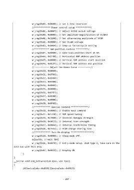
wr_reg(0x02, 0x0600); // set 1 line inversion
                             //************* Power control setup ************/
                             wr_reg(0x0C, 0x0007); // Adjust VCIX2 output voltage
                             wr_reg(0x0D, 0x0006); // Set amplitude magnification of VLCD63
                             wr_reg(0x0E, 0x3200); // Set alternating amplitude of VCOM
                             wr_reg(0x1E, 0x00BB); // Set VcomH voltage
                             wr_reg(0x03, 0x6A64); // Step-up factor/cycle setting
                             //************ RAM position control **********/
                             wr_reg(0x0F, 0x0000); // Gate scan position start at G0.
                             wr_reg(0x44, 0xEF00); // Horizontal RAM address position
                             wr_reg(0x45, 0x0000); // Vertical RAM address start position
                             wr_reg(0x46, 0x013F); // Vertical RAM address end position
                             // ----------- Adjust the Gamma Curve ----------//
                             wr_reg(0x30, 0x0000);
                             wr_reg(0x31, 0x0706);
                             wr_reg(0x32, 0x0206);
                             wr_reg(0x33, 0x0300);
                             wr_reg(0x34, 0x0002);
                             wr_reg(0x35, 0x0000);
                             wr_reg(0x36, 0x0707);
                             wr_reg(0x37, 0x0200);
                             wr_reg(0x3A, 0x0908);
                             wr_reg(0x3B, 0x0F0D);
                             //************* Special command **************/
                             wr_reg(0x28, 0x0006); // Enable test command
                             wr_reg(0x2F, 0x12EB); // RAM speed tuning
                             wr_reg(0x26, 0x7000); // Internal Bandgap strength
                             wr_reg(0x20, 0xB0E3); // Internal Vcom strength
                             wr_reg(0x27, 0x0044); // Internal Vcomh/VcomL timing
                             wr_reg(0x2E, 0x7E45); // VCOM charge sharing time
                             //************* Turn On display ******************/
                             wr_reg(0x10, 0x0000); // Sleep mode off.
                             delay(8); // Wait 30mS
                             wr_reg(0x11, 0x6878); // Entry mode setup. 262K type B, take care on the
             data bus with 16it only
                             wr_reg(0x07, 0x0033); // Display ON
                     }
             }
             __inline void LCD_SetCursor(u8 Xpos, u16 Ypos)
             {
                     if(DeviceCode==0x8999||DeviceCode==0x9919)


                                                         -  289  -