
Page 838 - 완) I MDP 프로젝트 작품 보고서(전체과 1학년)1.6
P. 838
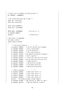
/* Enable clock for GPIOA,B,C,D,E AFIO and SPI3. */
               RCC->APB2ENR |= 0x0000007D;


               /* NCS is PB2, GPIO output set to high. */
               GPIOE->CRL = 0x33333333;
               GPIOE->CRH = 0x33333333;


               GPIOD->CRH &= 0x0000ffff;
               GPIOD->CRH |= 0x33330000;


               GPIOD->BSRR = 0x0000F000;             //cs,rs,wr,rd = 1;
               wr_reg(0x00, 0x0001);
               delay(2);                             /* Delay 50 ms */

              // DeviceCode = rd_reg(0x00);
               DeviceCode = 0x9325;
               if(DeviceCode == 0x9320)
               {
                       /* Start Initial Sequence --------------*/
                     wr_reg(0xE5, 0x8000);    /* Set the internal vcore voltage*/
                     wr_reg(0x00, 0x0001);    /* Start internal OSC*/
                     wr_reg(0x01, 0x0100);    /* Set SS and SM bit*/
                     wr_reg(0x02, 0x0700);    /* Set 1 line inversion*/
                     wr_reg(0x03, 0x1030);  /* Set GRAM write direction and BGR=1 */
                     wr_reg(0x04, 0x0000);   /* Resize register*/
                     wr_reg(0x08, 0x0202);  /* 2 lines each, back and front porch*/
                     wr_reg(0x09, 0x0000);  /* Set non-disp area refresh cyc ISC*/
                     wr_reg(0x0A, 0x0000);    /* FMARK function*/
                     wr_reg(0x0C, 0x0000);    /* RGB interface setting*/
                     wr_reg(0x0D, 0x0000);    /* Frame marker Position*/
                     wr_reg(0x0F, 0x0000);    /* RGB interface polarity*/


                       /* Power On sequence ----------------*/
                     wr_reg(0x10, 0x0000);    /* Reset Power Control 1*/
                     wr_reg(0x11, 0x0000);    /* Reset Power Control 2*/
                     wr_reg(0x12, 0x0000);    /* Reset Power Control 3*/
                     wr_reg(0x13, 0x0000);    /* Reset Power Control 4*/
                     delay(5);   /*Discharge cap power voltage (200ms)*/
                     wr_reg(0x10, 0x17B0);  /* SAP, BT[3:0], AP, DSTB, SLP, STB */
                     wr_reg(0x11, 0x0137);    /* DC1[2:0], DC0[2:0], VC[2:0]*/


                                                         -  831  -